
| Home | S-100 Boards | History | New Boards | Software | Boards For Sale |
| Forum | Other Web Sites | Quiz | Index |
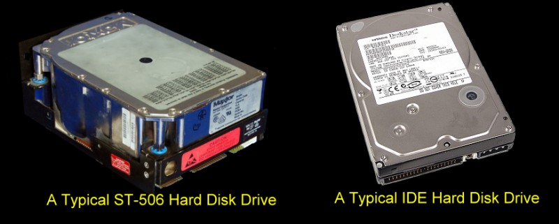
The IDE drive interface itself has a long history of incremental technical drive interface developments over the years. IDE evolved initially from Western Digitals hard drive interface used in the above IBM-AT. The central idea of the IDE interface was to place the drive controller, data separator etc. on the drive itself. This was a major improvement over the earlier ST-506 interfaces. It allowed for more drive construction possibilities, better standardization, better reliability and a more flexible connection to the computer itself. There were a number of improvements and name changes occurred over the years such as ATA/ATAPI. After the market introduction of Serial ATA in 2003, IDE/ATA interfaces were retroactively renamed Parallel ATA. I shall still use the term IDE here.
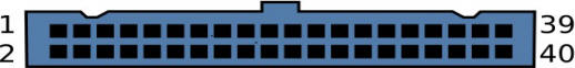
There are now actually two types of IDE connectors the "standard' 40 pin connector found on all IBM-PC type motherboards and a newer 44 pin connector used mainly in laptops for small laptop drives. The extra 4 pins are used to bring power (+5V) to the drive. Here is a picture of a standard IDE connector:-
Next install the two switches and only U2 and U3. We now will check port addressing. The board utilizes 74LS682's for port addressing. If your are unfamiliar with this technique click here.
Let’s assume you will be using the 4 port block 30H
to 33H. This is what I have the diagnostic software (MYIDE.ASM) port
defaults. We will set the 16 bit I/O address range to 00xxH by
jumpering K5 to 1-2 (the top two positions). Set switch SW2 positions 1-8 to
closed. Set
switch SW1 to 30-34H by having the switches (left to right):-
Open, closed, closed, open, open, closed, closed, closed.
Now put the card in your S-100 extender card and start the computer.
With your monitor at 0H in RAM enter:-
DB, 30, C3, 00, 00
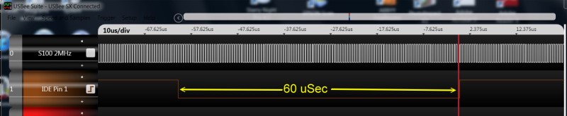
Jump to 0H. With a probe you should have pin 19 of U2 pulse continuously.
Do not go further until you see this.
Next add all the other IC’s except the 8255, U7 and U9. Note, U4 MUST be
a 74H04 or 74S04 (see below). The board will not work with IDE/CF cards with
a 74LS04. (It seems to be OK for slower Hard Disks with a 74LS04 chip).
Repeat the above software test. Check that pin 1 & 19 of empty socket of U9
for a pulse. It should not pulse for any other value except 30H, 31H, 32H, & 33H.
This insures we are able to read the data port correctly. Now the write to
ports test.
Same software as above except we have:-
D3, 30, C3, 00, 00
Check for a pulse on pins 1 & 19 of empty socket U7. Again it should
not pulse for any other value except 30H, 31H, 32H, & 33H
Only if you get this to work go further.
Insert the two 74LS244’s (U7 & U9) and the 8255.
We will now checkout the 8255. A complex chips with many configuration possibilities/modes. Fortunately for testing we need only the simplest mode where all 3 ports (A, B & C) are set as simple outputs. To do this from your monitor send to its control port (33H) the byte 80H. With this, port A (30H), port B (31H) and port C (32H) are configured for output ports.
With the LED’s on the board you can easily monitor port A.
Output to port C (32H), 0H. All the appropriate LED's should come on.
Then output 01, 02, 04, 08, 10H, 20H, 40H and 80H. The appropriate LED should
go off (see the above schematic).
Next we need to check port A (30H). Output to port 30H the value 0H. All the appropriate 8255 pins (4..1, 40..37) should be LOW. Then one at a time output a bit to this port. Starting at bit 0 send 01H to port 30H. See that pin 4 of the 8255 goes high. Continue all the way up to bit 7, pin 37 of the 8255.
Now do the same for the 8255 Port B (31H). First check the pins (18-25).
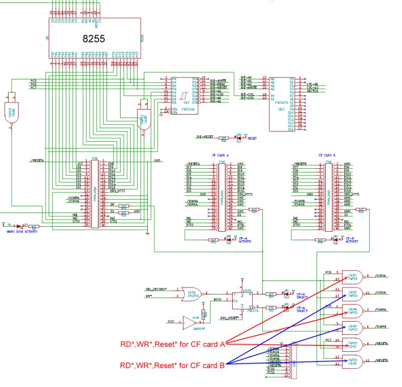
You will need a copy of the boards schematic. See
here.
Output to port 31H the value 0H. Pins 18-25 of the 8255 should be low. Output the
single bits pattern above and check each appropriate 8255 pin goes high.
Only if all of the above checks out should you go further.
Next we will check the actual IDE socket pins. Setup the 8255 to all ports
output as we did before (Output 80H to port 33H) then output to port 31H the
value 0H. ALL appropriate pins, 4,6…18 on any IDE socket should be 0. Then
output a 1 to port 31H. ONLY pin 4 on each IDE socket should be high. Same for all the other bits.
Only when you are sure that you can reliably output the correct bit pattern from
port 31H of the 8255 to any of the IDE sockets should you go further.
The boards are extremely well made so there is little chance of partial
etching. Any stuck bits are probably an error on your part.
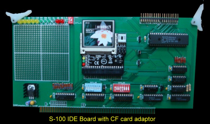
With the above completed, you are ready to fire things up with an IDE drive. I
have used the board with a number of drives and CF cards. I find it is
easiest to get things going with an old IDE hard drive. Be sure you plug
you plug the IDE cable in correctly. From the front of the board (V
regulators on left) the top IDE socket has pin 1 on the top row at the very
right back row of pins.
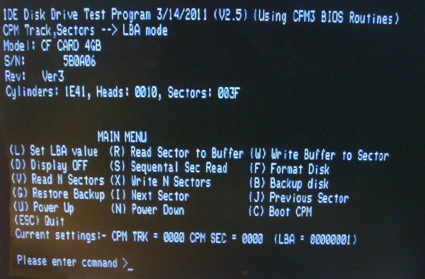
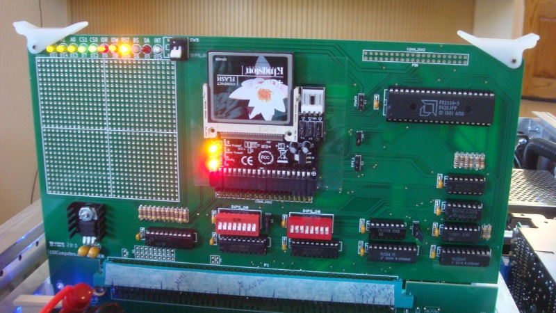
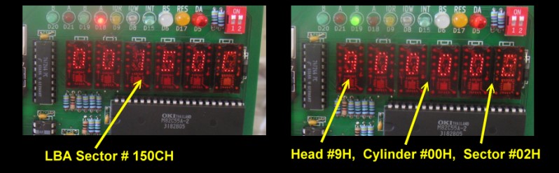
Download my “MYIDE.ASM” program to check things out. Run the program under CPM. The drive should come on and display the drive configuration parameters. See the picture above. The drive I used had 2082 cylinders, 16 heads and 63 sectors/track. You then need to read the sectors/track info you got and if required reassemble the program for your drive with the appropriate equates set in the software.
As I said, I have two of these new boards running here (on two systems).
They appear very reliable. I have extensively slopped large files to/from
memory disks and down to slow floppies. Never a problem. It’s so nice to
instantly have CPM3 boot up!
The only unusual thing I have found is the requirement of U4 being a fast
74H04 or 74S04 when using CF disks. It’s an absolute requirement for
the cards I have. Not so for regular hard disks. I have not really
determined why this is the case.
You can "Hot Swap" the CF cards in a running CPM system if you first turn off power to the IDE adaptor/CF board (SW3), remove the CF card. Insert the new card and THEN turn the power back on with switch SW3. With CPM you need to warm boot with a ^C. Clearly there must be a system on the new CF card or you must do the swap where another drive is the current system drive.
Software
.jpg)
AH = 02h
AL = number of sectors to read/written (must be nonzero)
CH = low eight bits of cylinder number
CL = sector number 1-63 (bits 0-5)
high two bits of cylinder (bits 6-7, hard disk only)
DH = head number
DL = drive number (bit 7 set for hard disk)
ES:BX -> data buffer
Because only 16 heads are allowed with this format, a hard disk can only get to 512MG in size. This is not a problem for 8 bit CPM systems since disk capacity was always less than 10 MG. To go to higher disk capacities with later version of MSDOS, the PC BIOS's utilized the so called "LBA" sector addressing mode. In this case sectors are numbered on the disk as just one long number. Starting at 0 and working upwards. There are no tracks or heads. Both formats can be implemented on our IDE board.
| Bit 7 | Bit 6 | Bit 5 | Bit 4 | Bit 3 | Bit2 | Bit 1 | Bit 0 |
| Always 1 | LBA/CHS mode | Always 1 | M/Slave | Heads 0-15 | |||
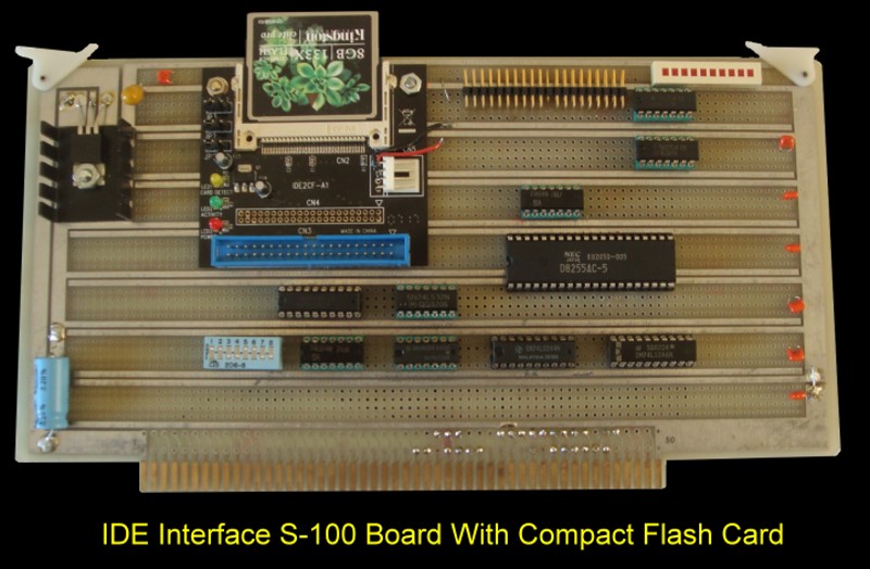
A Final Dual IDE
Prototype Board
Utilizing all the observations above Andrew and I constructed one more
prototype board to make sure everything is correct for what we expect will
be a popular S-100 board. Here is a picture of that board:-
.jpg)
Added where more LED's to let you know which CF card/drive is selected and
when a drive is active (RD/WR). The board works fine with 7403's rather than
the less common 74F03's. It also works fine with the low power CMOS 82C55's
or the older plain NMOS 8255's.
It is interesting to go back and see how this board has evolved.
It now has become a fairly sophisticated board and very useful.
These days I store everything on CF cards!
If you have an interest in such a bare board, let Andrew know via e-mail at:-
lynchaj@yahoo.com .
Please note all the above
clearly applies only to people who know what they are doing and can do
a little soldering and board assembly. There will be little hand holding
at this stage.
A Production Version of the DUAL IDE Board
Because this board and software may be of use to others, together with Andrew Lynch at N8VEM (see
here) we made a
"proper" commercial type S-100 V2 board. Shown below. The board uses
24 bit address lines and 16 or 8 bit IO ports. The construction
process is more or less the same as that described for the V1 board above,
however do consult the schematic as the IC numbers etc. have changed.
You can see we added a second Voltage regulator. The single regulator was
running a little hot on the final prototype. Now the LED HEX display has its
own 5V regulator.
.jpg)
Source of chips
Most of the IC's use on this board are common 74LSxx chips available from
numerous sources such a Jameco, Mouser & DigiKey.
The TIL 311A's are
expensive (~$20 each from places like Jameco). However overseas
outfits like
Utsource sell them in small quantities for ~$5 each. Utsource have about
a 1 week delivery time to the US since they use DHL. It is indeed
frustrating these LED HEX displays are so expensive. With the exception of
the even rarer HP-5082's other
such displays display only the digits 0-9. An alternative approach
would be to use a 7 segment LED decoder such as a
DM9368 and a simple
7 segment LED display. However these too are no longer normally stocked.
Normal single line flat panel LCD displays just do not show up well when the
card is in the S-100 bus card cage.
The links below will contain the most recent schematic of this board.
Note, it may change over time and some IC part or pin numbers may not correlate
exactly with the text in the article above.
This page was last modified on 09/18/2011